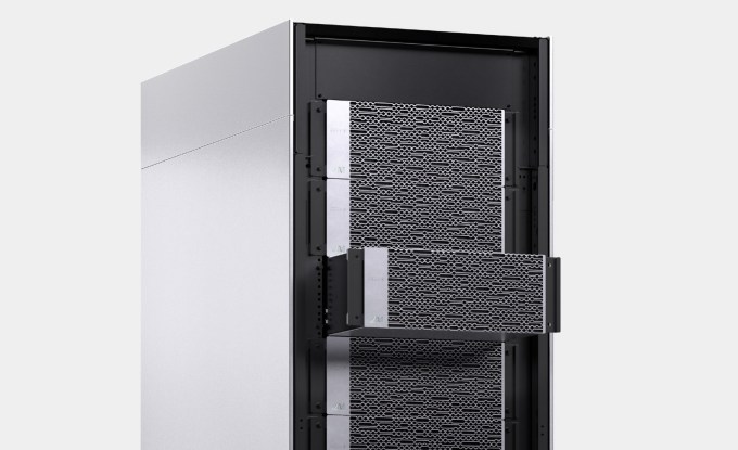
Photonic computing startup Lightmatter has raised $400 million to blow one of modern data centers’ bottlenecks wide open. The company’s optical interconnect layer allows hundreds of GPUs to work synchronously, streamlining the costly and complex job of training and running AI models.
The growth of AI and its correspondingly immense compute requirements have supercharged the data center industry, but it’s not as simple as plugging in another thousand GPUs. As high-performance computing experts have known for years, it doesn’t matter how fast each node of your supercomputer is if those nodes are idle half the time waiting for data to come in.
The interconnect layer or layers are really what turn racks of CPUs and GPUs into effectively one giant machine — so it follows that the faster the interconnect, the faster the data center. And it is looking like Lightmatter builds the fastest interconnect layer by a long shot, by using the photonic chips it’s been developing since 2018.
“Hyperscalers know if they want a computer with a million nodes, they can’t do it with Cisco traditional switches. Once you leave the rack, you go from high-density interconnect to basically a cup on a string,” Nick Harris, CEO and founder of the company, told TechCrunch. (You can see a short talk he gave summarizing this issue here.)
The state of the art, he said, is NVLink and particularly the NVL72 platform, which puts 72 Nvidia Blackwell units wired together in a rack, capable of a maximum of 1.4 exaFLOPs at FP4 precision. But no rack is an island, and all that compute has to be squeezed out through 7 terabits of “scale up” networking. Sounds like a lot, and it is, but the inability to network these units faster to each other and to other racks is one of the main barriers to improving performance.
“For a million GPUs, you need multiple layers of switches, and that adds a huge latency burden,” said Harris. “You have to go from electrical to optical to electrical to optical… the amount of power you use and the amount of time you wait is huge. And it gets dramatically worse in bigger clusters.”
So what’s Lightmatter bringing to the table? Fiber. Lots and lots of fiber, routed through a purely optical interface. With up to 1.6 terabits per fiber (using multiple colors), and up to 256 fibers per chip… well, let’s just say that 72 GPUs at 7 terabits starts to sound positively quaint.
“Photonics is coming way faster than people thought — people have been struggling to get it working for years, but we’re there,” said Harris. “After seven years of absolutely murderous grind,” he added.
The photonic interconnect currently available from Lightmatter does 30 terabits, while the on-rack optical wiring is capable of letting 1,024 GPUs work synchronously in their own specially designed racks. In case you’re wondering, the two numbers don’t increase by similar factors because a lot of what would need to be networked to another rack can be done on-rack in a thousand-GPU cluster. (And anyway, 100 terabit is on its way.)

The market for this is huge, Harris pointed out, with every major data center company from Microsoft to Amazon to newer entrants like xAI and OpenAI showing an endless appetite for compute. “They’re linking together buildings! I wonder how long they can keep it up,” he said.
Many of these hyperscalers are already customers, though Harris wouldn’t name any. “Think of Lightmatter a little like a foundry, like TSMC,” he said. “We don’t pick favorites or attach our name to other people’s brands. We provide a roadmap and a platform for them — just helping grow the pie.”
But, he added coyly, “you don’t quadruple your valuation without leveraging this tech,” perhaps an allusion to OpenAI’s recent funding round valuing the company at $157 billion, but the remark could just as easily be about his own company.
This $400 million D round values it at $4.4 billion, a similar multiple of its mid-2023 valuation that “makes us by far the largest photonics company. So that’s cool!” said Harris. The round was led by T. Rowe Price Associates, with participation from existing investors Fidelity Management & Research Company and GV.
What’s next? In addition to interconnect, the company is developing new substrates for chips so that they can perform even more intimate, if you will, networking tasks using light.
Harris speculated that, apart from interconnect, power per chip is going to be the big differentiator going forward. “In 10 years you’ll have wafer-scale chips from everybody — there’s just no other way to improve the performance per chip,” he said. Cerebras is of course already working on this, though whether they are able to capture the true value of that advance at this stage of the technology is an open question.
But for Harris, seeing the chip industry coming up against a wall, he plans to be ready and waiting with the next step. “Ten years from now, interconnect is Moore’s Law,” he said.


Leave a Reply